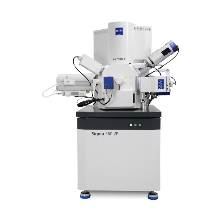
ZEISS Sigma 500 电子显微镜
制造商: ZEISS Model: Sigma 500 来源: Germany - 联系
Electron Source: Schottky Thermal Field Emitter Schottky Thermal Field Emitter
Resolution* at 30 kV (STEM): 0.8 nm
Resolution* at 15 kV: 0.7 nm
Resolution* at 1 kV: 1.2 nm
Resolution at 500 V: 1.5 nm
Resolution* at 30 kV: (VP Mode) 1.5 nm
Accelerating Voltage: 0.02 – 30 kV
Magnification: 12× – 1,000,000×
Field of View: 4.6 mm
Probe Current 3 pA - 20 nA (100 nA optional)
Image Framestore: 32 k × 24 k pixels
Type of Diode: Silicon based diode for direct detection of backscattered electrons, one segment
Image Polarity: Configurable. Default: “TEM” like contrast
Optimum Working Distance: 4 – 6 mm
Energy Range: < = 7 keV
Optimum Primary Beam Current: 50 pA – 1nA
Mechanical Module: Highly stable mechanical module with acoustic dampening cover
Easy Servicability: Diode exchange is plug & play
Protection:
Protective cover to avoid charging and damage to the diode.
Integrated protection during plasma cleaning of sample/chamber.
Lifetime: Expected lifespan of detector diode: 2 years under average usage conditions
System Integration:
Collision control with ZEISS hardware implemented.
Acceleration voltage limited to <7 kV.
EO table correction is applied.
User Interface: Default settings optimized for ease of use.
Insertion and Retraction: Pneumatic
- 质量承诺
- 正品保修
- 送货到家
- 交易简单化